2. Komponen [back]
| No | Nama Alat | Spesifikasi | Jumlah |
| 1 | Gambar layout komponen | 1 set | |
| 2 | Ground | 1 set | |
| 3 | power | 1 buah | |
| 4 | Solder | 1 buah | |
| 5 | Penyedot timah | 1 buah | |
| 6 | Tang potong | 1 buah | |
| 7 | Tang lancip | 1 buah | |
| 8 | Mistar baja | 1 buah | |
| 9 | Landasan solder | 1 buah | |
| 10 | Mata bor | 1 buah |


3.Dasar Teori [back]
1.I've been reviewing some past exam and stumbled across this question

So I need to find the current I through the middle diode and the voltage across the bottom left 10KΩ resistor.
Solution
I think the easiest method to solve such problems is to assume that the diodes are off (both, and then one of the two), compute the voltages across the diodes and see if there's a contradiction with your assumption. Let's call the top left diode and the diode in the middle .
Case 1: off, off: Since is off there is no current through the top 5k resistor, and since is off, there is also no current through the bottom left 10k resistor. So and the voltage at the anode of is 15 Volts. Contradiction! ( should be on).
Case 2: off, on: again no current through top 5k resistor. Voltage is
Contradiction! (Because the voltage across would be and it should be on.)
Case 3: on, off: Voltage is
The voltage at the anode of is . This agrees with our assumption, because with these voltages must be off. So your solution is
I=0A,V=10VI=0A,V=10V
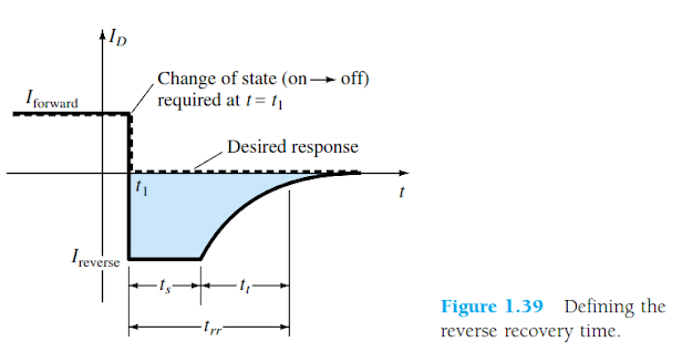
2.What is the reverse recovery time in a diode?
Solution
If a diode is conducting in a forward condition and immediately switched to a reverse condition, the diode will conduct in a reverse condition for a short time as the forward voltage bleeds off. The current through the diode will be fairly large in a reverse direction during this small recovery time.
After the carriers have been flushed and the diode is acting as a normal blocking device in the reversed condition, the current flow should drop to leakage levels.
The charge flowing during reverse recovery time is called "reverse recovery charge" and the diode has to extinguish it ("recovery" from reverse-biased to neutral condition) before you can turn it on. In the end, reverse recovery phenomenon depends on silicon doping and geometry and is a parasitic effect in diodes, because energy involved in the process is lost. strong text
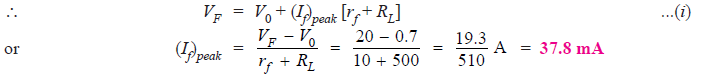
1. An a.c. voltage of peak value 20 V is connected in series with a silicon diode and
load resistance of 500 Ω. If the forward resistance of diode is 10 Ω, find :
(i) peak current through diode (ii) peak output voltage
What will be these values if the diode is assumed to be ideal ?
Solution :
Peak input voltage = 20 V
Forward resistance, rf = 10 Ω
Load resistance, RL= 500 Ω
Potential barrier voltage, V0 = 0.7 V
The diode will conduct during the positive half-cycles of a.c. input voltage only.
The equivalent circuit is shown in Fig.1(ii)
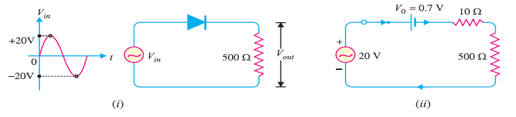
Fig. 1
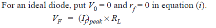
(i) The peak current through the diode will occur at the instant when the input voltage reaches positive peak i.e. Vin = VF = 20 V.
(ii) Peak output voltage : Ideal Diode Case:

Peak input voltage = 20 V
Forward resistance, rf = 10 Ω
Load resistance, RL= 500 Ω
Potential barrier voltage, V0 = 0.7 V
The diode will conduct during the positive half-cycles of a.c. input voltage only.
The equivalent circuit is shown in Fig.1(ii)
Fig. 1
(i) The peak current through the diode will occur at the instant when the input voltage reaches positive peak i.e. Vin = VF = 20 V.
(ii) Peak output voltage :![]() Ideal Diode Case:
Ideal Diode Case:
2. Determine the state of diode for the circuit shown in Fig. 10 (i) and find ID and VD . Assume simplified model for the diode.
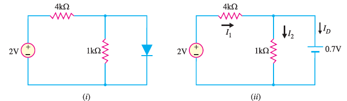
Fig. 10
Fig. 10
Solution :
Let us assume that the diode is ON. Therefore, we can replace the diode with a 0.7V battery as shown in Fig. 10 (ii). Referring to Fig.10 (ii), we have,
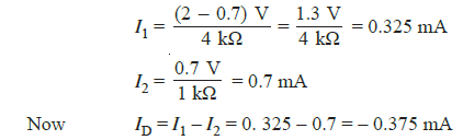
Since the diode current is negative, the diode must be OFF and the true value of diode current is ID =0 mA. Hence our initial assumption was wrong.
In order to analyse the circuit properly, we should replace the diode in Fig. 10 (i) with an open circuit as shown in Fig.10(iii).
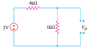
Fig.10 (iii)
The voltage VD across the diode is :
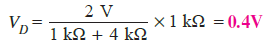
We know that 0.7V is required to turn ON the diode. Since VD is only 0.4V, the answer confirms that the diode is OFF.
Let us assume that the diode is ON. Therefore, we can replace the diode with a 0.7V battery as shown in Fig. 10 (ii). Referring to Fig.10 (ii), we have,
Since the diode current is negative, the diode must be OFF and the true value of diode current is ID =0 mA. Hence our initial assumption was wrong.
In order to analyse the circuit properly, we should replace the diode in Fig. 10 (i) with an open circuit as shown in Fig.10(iii).
Fig.10 (iii)
The voltage VD across the diode is :
We know that 0.7V is required to turn ON the diode. Since VD is only 0.4V, the answer confirms that the diode is OFF.
1.Apa syarat suatu diode dikatakan "off"?

A.ketika ID = 0
B.Ketika VD > 0
C.Ketika VD <0
D.Ketika ID >0
E.Ketika Iforward > Ireverse
2. Perhatikan Gambar berikut

A. Diode 1 OFF Diode 2 OFF
B. Diode 1 OFF Diode 2 ON
C. Diode 1 ON Diode 2 OFF
D. Diode 1 ON Diode 2 ON
Solution


Step 3: BUAT SIMULASI PADA PROTEUS


Ketika Switch dipindahkan dari "ON" ke "OFF"

Ketika Switch dipindahkan dari "OFF" ke "ON"


Reverse Recovery Time dipengaruhi oleh besarnya tegangan sumber. Semakin besar tegangannya maka Nilai dari trr nya juga semakin besar. atau ibaratnya seperti lampu dalam kehidupan kita sehari-hari.ada beberapa kasus dimana lampu yang awalnya hidup, ketika dimatikan ia tidak langsung padam, tapi ia redup sebentar baru padam.begitu pula dengan dioda,dalam dioda ada yang namanya arus forward(Iforward) dan ada yang namanya arus reverse(Ireverse). Iforward (yaitu ketika arus yang mengalir dari kutub positif sumber menuju anode dioda,maka dioda akan "on") dan Ireverse (yaitu ketika arus yang mengalir dari kutub positif sumber menuju katode dioda,maa dioda akan "off").

Tidak ada komentar:
Posting Komentar